
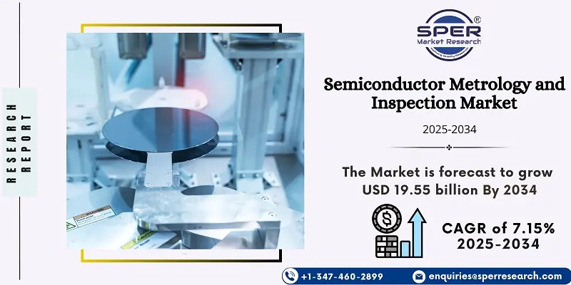
Semiconductor Metrology and Inspection Market Size 2034
Semiconductor Metrology and Inspection Market Growth, Size, Trends Analysis – By Type, By Technology, By Application- Regional Outlook, Competitive Strategies and Segment Forecast to 2034
| Published: Sep-2025 | Report ID: SEMI2577 | Pages: 1 - 251 | Formats*: |
| Category : Semiconductor and Electronics | |||
| Report Metric | Details |
| Market size available for years | 2021-2034 |
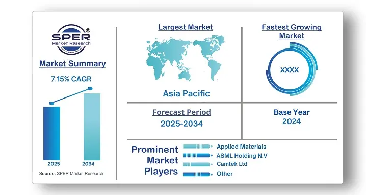
| Base year considered | 2024 |
| Forecast period | 2025-2034 |
| Segments covered | By Type, By Technology, By Application |
| Regions covered | North America, Latin America, Asia-Pacific, Europe, and Middle East & Africa |
| Companies Covered | Applied Materials, Inc., ASML Holding N.V., Camtek Ltd., Hitachi Ltd., KLA Corporation, Onto Innovation, Inc., and Thermo Fisher Scientific Inc |
- Global Semiconductor Metrology and Inspection Market Size (FY 2021-FY 2034)
- Overview of Global Semiconductor Metrology and Inspection Market
- Segmentation of Global Semiconductor Metrology and Inspection Market by Type (Water Inspection System, Mask Inspection System, Thin Film Metrology, Bump Inspection, Load Frame Inspection)
- Segmentation of Global Semiconductor Metrology and Inspection Market by Technology (Optical, E-Bean, Others)
- Segmentation of Global Semiconductor Metrology and Inspection Market by Application (Integrated Circuit Manufacturing, Light Emitting Diode (LED) Manufacturing, Discrete Devices, Packaging and Assembly, Others)
- Statistical Snap of Global Semiconductor Metrology and Inspection Market
- Expansion Analysis of Global Semiconductor Metrology and Inspection Market
- Problems and Obstacles in Global Semiconductor Metrology and Inspection Market
- Competitive Landscape in the Global Semiconductor Metrology and Inspection Market
- Details on Current Investment in Global Semiconductor Metrology and Inspection Market
- Competitive Analysis of Global Semiconductor Metrology and Inspection Market
- Prominent Players in the Global Semiconductor Metrology and Inspection Market
- SWOT Analysis of Global Semiconductor Metrology and Inspection Market
- Global Semiconductor Metrology and Inspection Market Future Outlook and Projections (FY2025-FY 2034)
- Recommendations from Analyst
- 1.1. Scope of the report
- 1.2. Market segment analysis
- 2.1. Research data source
- 2.1.1. Secondary Data
- 2.1.2. Primary Data
- 2.1.3. SPERs internal database
- 2.1.4. Premium insight from KOLs
- 2.2. Market size estimation
- 2.2.1. Top-down and Bottom-up approach
- 2.3. Data triangulation
- 4.1. Driver, Restraint, Opportunity and Challenges analysis
- 4.1.1. Drivers
- 4.1.2. Restraints
- 4.1.3. Opportunities
- 4.1.4. Challenges
- 5.1. SWOT Analysis
- 5.1.1. Strengths
- 5.1.2. Weaknesses
- 5.1.3. Opportunities
- 5.1.4. Threats
- 5.2. PESTEL Analysis
- 5.2.1. Political Landscape
- 5.2.2. Economic Landscape
- 5.2.3. Social Landscape
- 5.2.4. Technological Landscape
- 5.2.5. Environmental Landscape
- 5.2.6. Legal Landscape
- 5.3. PORTERs Five Forces
- 5.3.1. Bargaining power of suppliers
- 5.3.2. Bargaining power of buyers
- 5.3.3. Threat of Substitute
- 5.3.4. Threat of new entrant
- 5.3.5. Competitive rivalry
- 5.4. Heat Map Analysis
- 6.1. Semiconductor Metrology and Inspection Market Manufacturing Base Distribution, Sales Area, Product Type
- 6.2. Mergers & Acquisitions, Partnerships, Product Launch, and Collaboration in Global Semiconductor Metrology and Inspection Market
- 7.1. Water Inspection System
- 7.2. Mask Inspection System
- 7.3. Thin Film Metrology
- 7.4. Bump Inspection
- 7.5. Load Frame Inspection
- 8.1. Optical
- 8.2. E-Bean
- 8.3. Others
- 9.1. Integrated Circuit Manufacturing
- 9.2. Light Emitting Diode (LED) Manufacturing
- 9.3. Discrete Devices
- 9.4. Packaging and Assembly
- 9.5. Others
- 10.1. Global Semiconductor Metrology and Inspection Market Size and Market Share
- 11.1. Asia-Pacific
- 11.1.1. Australia
- 11.1.2. China
- 11.1.3. India
- 11.1.4. Japan
- 11.1.5. South Korea
- 11.1.6. Rest of Asia-Pacific
- 11.2. Europe
- 11.2.1. France
- 11.2.2. Germany
- 11.2.3. Italy
- 11.2.4. Spain
- 11.2.5. United Kingdom
- 11.2.6. Rest of Europe
- 11.3. Middle East and Africa
- 11.3.1. Kingdom of Saudi Arabia
- 11.3.2. United Arab Emirates
- 11.3.3. Qatar
- 11.3.4. South Africa
- 11.3.5. Egypt
- 11.3.6. Morocco
- 11.3.7. Nigeria
- 11.3.8. Rest of Middle-East and Africa
- 11.4. North America
- 11.4.1. Canada
- 11.4.2. Mexico
- 11.4.3. United States
- 11.5. Latin America
- 11.5.1. Argentina
- 11.5.2. Brazil
- 11.5.3. Rest of Latin America
- 12.1. Applied Materials, Inc.
- 12.1.1. Company details
- 12.1.2. Financial outlook
- 12.1.3. Product summary
- 12.1.4. Recent developments
- 12.2. ASML Holding N.V.
- 12.2.1. Company details
- 12.2.2. Financial outlook
- 12.2.3. Product summary
- 12.2.4. Recent developments
- 12.3. Camtek Ltd.
- 12.3.1. Company details
- 12.3.2. Financial outlook
- 12.3.3. Product summary
- 12.3.4. Recent developments
- 12.4. Hitachi Ltd.
- 12.4.1. Company details
- 12.4.2. Financial outlook
- 12.4.3. Product summary
- 12.4.4. Recent developments
- 12.5. KLA Corporation
- 12.5.1. Company details
- 12.5.2. Financial outlook
- 12.5.3. Product summary
- 12.5.4. Recent developments
- 12.6. Onto Innovation, Inc.
- 12.6.1. Company details
- 12.6.2. Financial outlook
- 12.6.3. Product summary
- 12.6.4. Recent developments
- 12.7. Thermo Fisher Scientific Inc.
- 12.7.1. Company details
- 12.7.2. Financial outlook
- 12.7.3. Product summary
- 12.7.4. Recent developments
- 12.8. Others
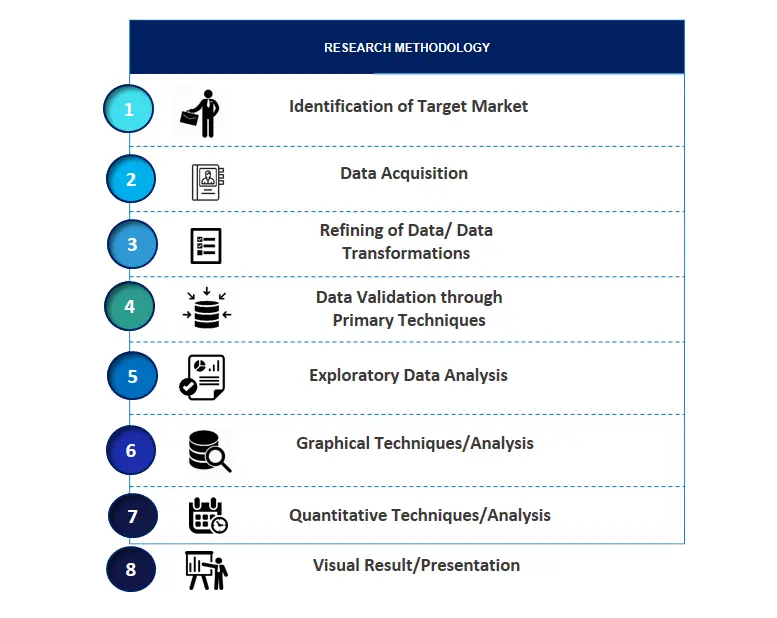
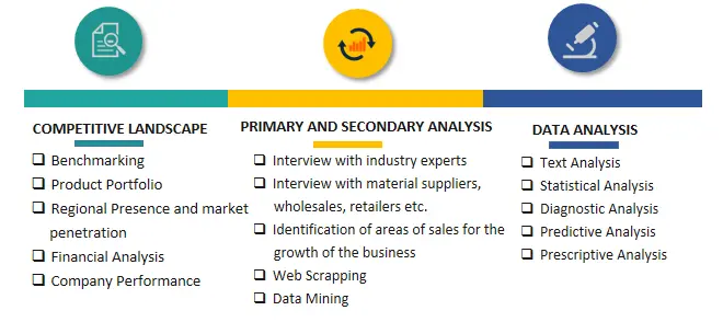
SPER Market Research’s methodology uses great emphasis on primary research to ensure that the market intelligence insights are up to date, reliable and accurate. Primary interviews are done with players involved in each phase of a supply chain to analyze the market forecasting. The secondary research method is used to help you fully understand how the future markets and the spending patterns look likes.
The report is based on in-depth qualitative and quantitative analysis of the Product Market. The quantitative analysis involves the application of various projection and sampling techniques. The qualitative analysis involves primary interviews, surveys, and vendor briefings. The data gathered as a result of these processes are validated through experts opinion. Our research methodology entails an ideal mixture of primary and secondary initiatives.
Frequently Asked Questions About This Report
PLACE AN ORDER
Year End Discount
Sample Report
Pre-Purchase Inquiry
NEED CUSTOMIZATION?
Request CustomizationCALL OR EMAIL US
100% Secure Payment